선택적 증착
복잡한 패터닝 설계, 더 높은 종횡비, 더 작은 비아 및 채널, 더 취약한 형상, 증가하는 패턴 붕괴의 위험으로 인해 벌크 재료 엔지니어링에서 선택적 공정으로 빠르게 전환되고 있습니다.
선택적 공정은 특별히 공동 설계된 화학 물질 및 재료 상호작용을 사용하여 대상 재료의 섬세하고 정확한 증착과 제거를 가능하게 합니다. 선택적 증착은 원자 단위의 적층 가공으로, 원자를 필요한 곳에만 배치합니다. 선택적 제거는 원자 단위의 절삭 가공으로, 가시 범위 내에 있는지 여부에 상관없이 원치 않는 원자만 제거하고 나머지는 그대로 남겨둡니다. 선택적 식각 및 증착 기술을 사용하여 작은 패턴을 생성 및 형성하고 새로운 구조를 제작할 수 있으며, 습식 공정과 관련된 패턴 붕괴, 패터닝 시 가장자리 배치 문제, 트랜지스터 컨택 및 인터커넥트 저항과 관련된 2D 미세화 문제 등과 같은 기술적 장애물을 극복할 수 있습니다.
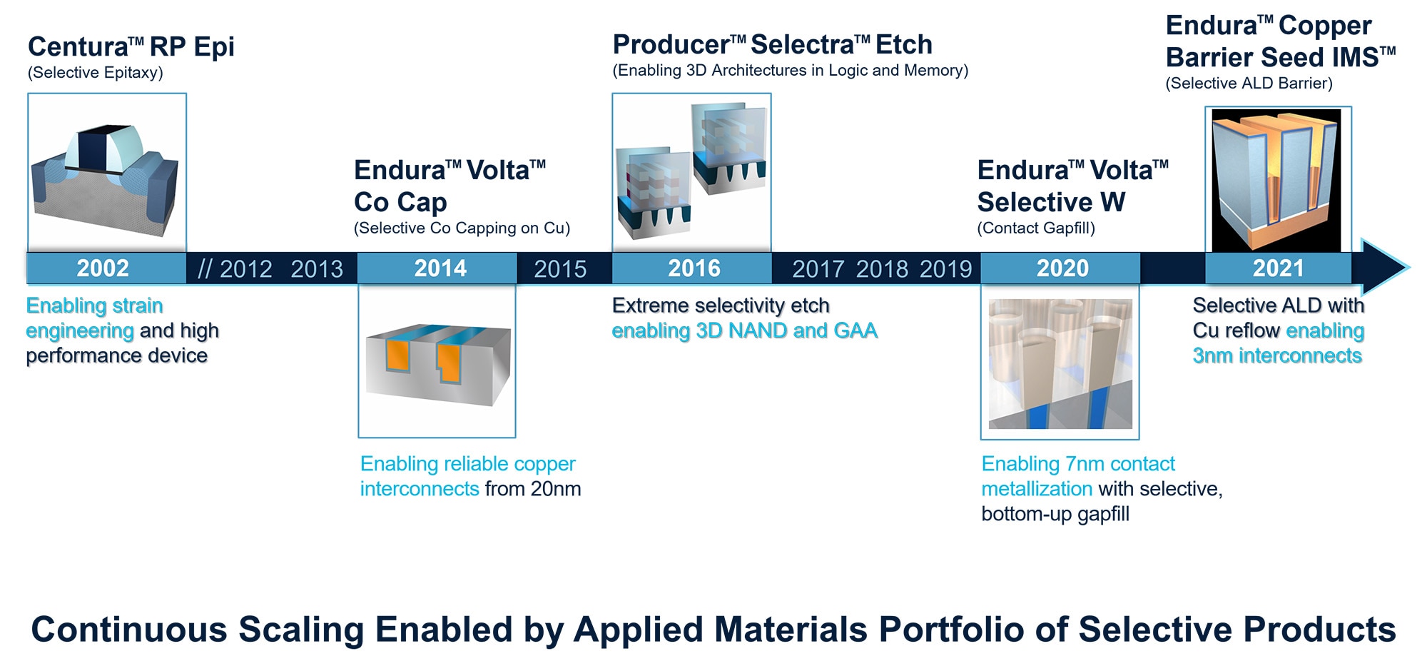
Applied leads the industry in selective deposition and selective epitaxy processes. The Endura Copper Barrier Seed IMS™ replaces standard high-resistance via interfaces with a low-resistance selective ALD barrier to enable interconnect metallization for 3nm and beyond. Similarly, the Endura Volta Selective W CVD system replaces conventional metal and dielectric liners and barriers with selective Tungsten deposition to lower contact resistivity and reduce the bottleneck of 2D scaling. The Endura Volta CVD Cobalt system provides a robust seed layer for copper lines and selective Cobalt cap to strengthen adhesion at the copper-dielectric interface. Finally, the Centura Prime Epi system plays a critical role in strain engineering Si-Ge channel performance found in FinFET and GAA transistors.