인터커넥트
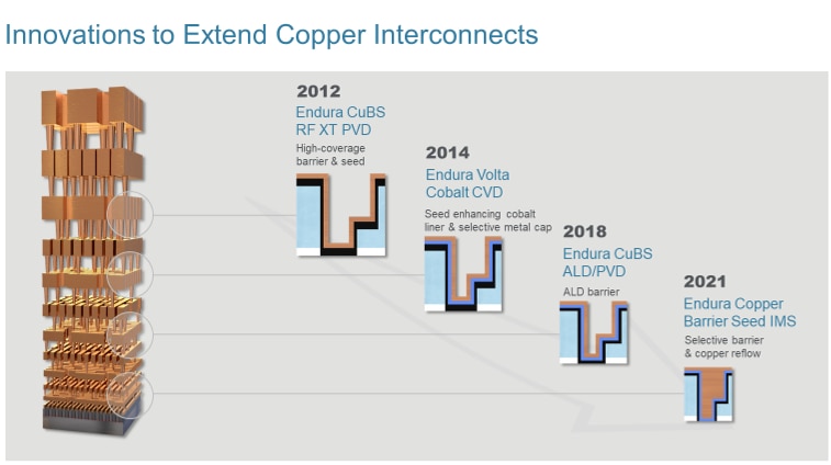
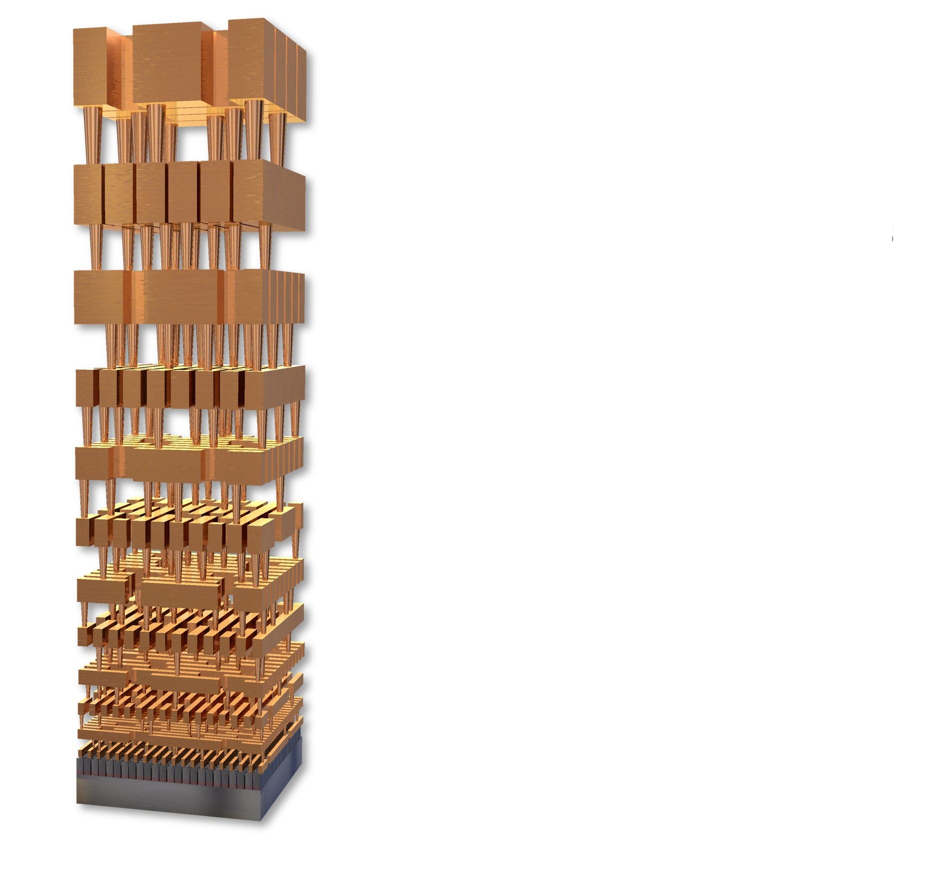
Logic scaling requires more than shrinking transistor size alone—innovations in the transistor contact and chip interconnect modules are necessary as well. A smartphone processor has over 16 billion transistors and over 32 billion via and contact connections. 게다가 10개가 넘는 다양한 치수의 금속 레이어가 있으며, 트랜지스터에 가장 가까운 레이어의 폭이 가장 좁습니다.
Transistors, which act as switches, are connected electrically through metal contacts that are then interconnected by copper wires, or copper interconnects. 이러한 인터커넥트는 전력을 분배하고 로직 신호를 라우팅합니다. As transistor dimensions shrink, interconnect resistance increases dramatically, impacting device power and performance, necessitating continuous advances in materials and process technologies.
As the leader in interconnect process technology, Applied Materials enables innovations in this area with our successful suite of products in metals deposition. 인 선택적 장벽층 증착 및 구리 리플로우 기술을 갖춘 Endura® Copper Barrier IMS® 시스템은 3nm 미만의 로직 스케일링을 지속하는 데 필수적인 접점과 상호 연결을 구현하는 데 매우 중요합니다.
2nm 노드를 뛰어넘는 미세화를 지속하려면 공정 기술뿐만 아니라 인터커넥트 및 컨택에서의 주요 혁신이 필수입니다. 후면 전력 공급이 그러한 혁신 중 하나입니다.