Products & Technologies
Products & Services
Contact
Products & Services
Products & Technologies
Services
Resources
Contact
Innovation and Commercialization
The EPIC Advanced Packaging Center in Singapore is designed to accelerate innovation and commercialization of advanced packaging technologies and marks the next phase of building out Applied’s global EPIC Platform.
The center brings together the necessary components to enable the next generation of energy-efficient computing for the AI era and builds upon the strong foundation of the Advanced Packaging Development Center (APDC), a decade-long collaboration between Applied Materials and Singapore’s Institute of Microelectronics (IME).
The EPIC Advanced Packaging Center innovation model will accelerate the time to innovation and shorten the time to commercialization.
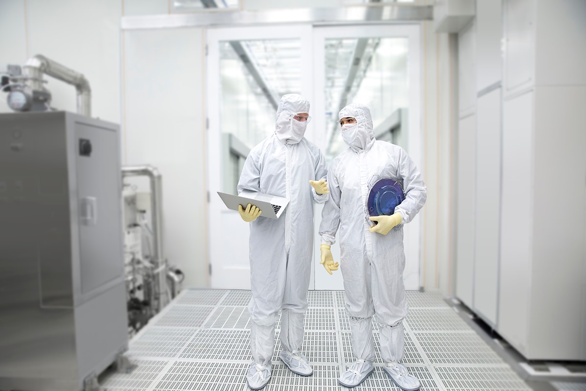
Among the most advanced wafer-level packaging labs in the world, this facility enables innovation of the foundational building blocks of advanced packaging, including advanced bump and micro-bump, fine-line redistribution layer (RDL), through-silicon via (TSV) and hybrid bonding.
Dedicated Packaging Ecosystem
The center greatly expands Applied’s infrastructure for advanced packaging R&D and will include dedicated private spaces for customers and partners as well as a dedicated pilot line of packaging process equipment to enable test vehicles and prototype production.
Introduction to Testimonials
First Last
CEO, Company name