Unique Approach to Ecosystem Collaboration
EPIC is Equipment and Process Innovation and Commercialization
The EPIC model provides a collaborative foundation, which allows the ecosystem to anticipate inflections and deliver solutions critical to competitive advantage in fast-growing markets. Our physical and digital networks within the EPIC model will drive the foundational technologies that define how future chips are made and create the future innovation and manufacturing talent pipeline. Applied developed this new way of collaborating in response to our customers and partners need to more rapidly access next-generation technologies and solutions to advance chipmaking.
High Velocity Innovation and Commercialization
The Internet of Things (IoT) and artificial intelligence (AI) demand rapid, dramatic improvements in chip performance, power, area, cost and time to market, which we call PPACt. Applied Materials is committed to accelerating this new playbook for our customers and partners. With the broadest and deepest portfolio of products for delivering materials engineering innovations to the market, Applied Materials is committed to accelerating high velocity co-innovation.
Learn More About Our EPIC Centers
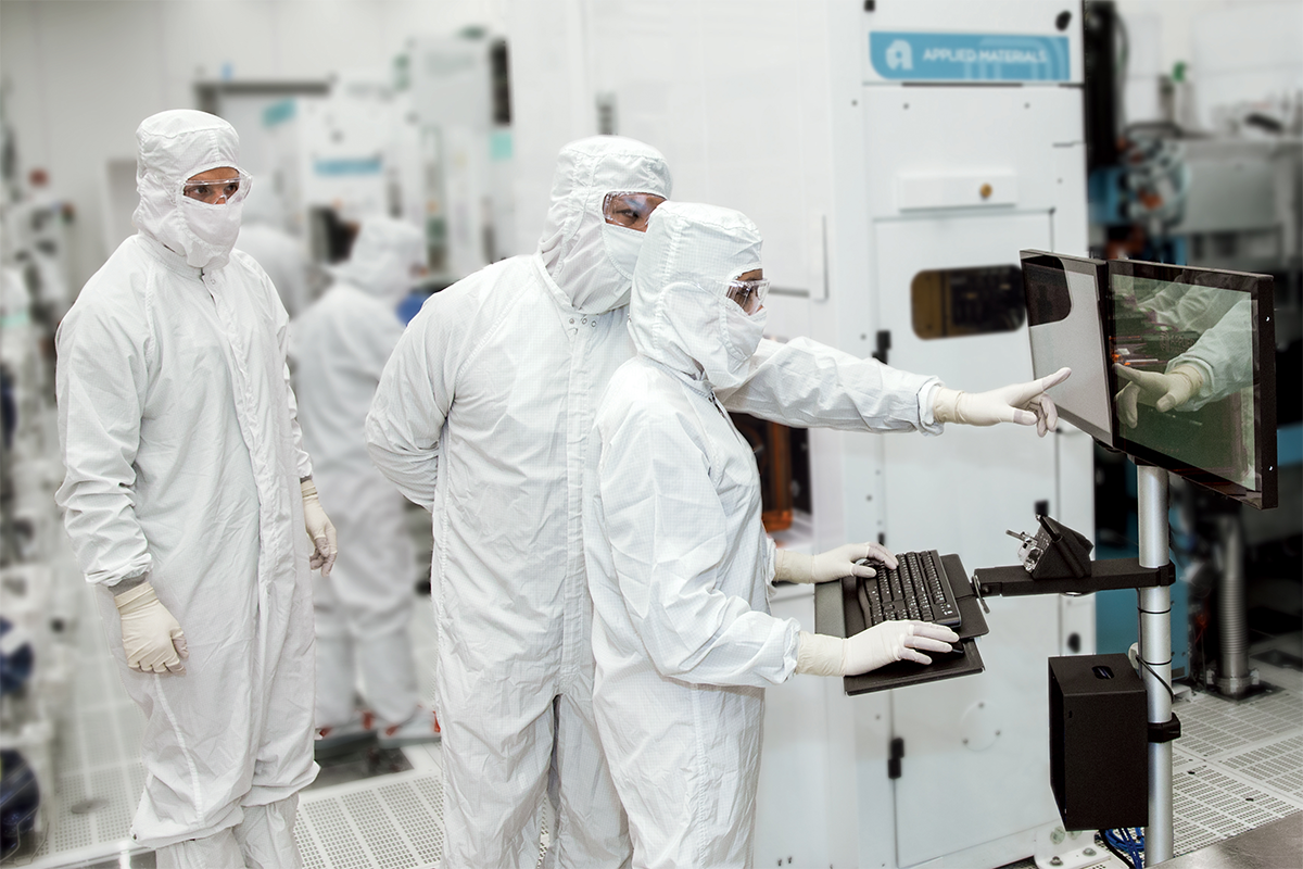
EPIC Center Silicon Valley

Rendering of the future Applied Materials Equipment and Process Innovation and Commercialization (EPIC) Center.
EPIC Center – Expected in 2026
The new Equipment and Process Innovation and Commercialization (EPIC) Center is planned as the heart of a high-velocity innovation platform designed to accelerate development and commercialization of the foundational technologies needed by the global semiconductor and computing industries. To be located at the Applied campus in Sunnyvale, California, the multibillion-dollar facility is designed to provide a breadth and scale of capabilities that is unique in the industry, including more than 180,000 square feet of state-of-the-art cleanroom for collaborative innovation with chipmakers, universities and ecosystem partners. Designed from the ground up to accelerate the pace of introducing new manufacturing innovations, the new EPIC Center is expected to reduce the time it takes the industry to bring a technology from concept to commercialization by several years, while simultaneously increasing the commercial success rate of new innovations and the return on R&D investments for the entire semiconductor ecosystem.
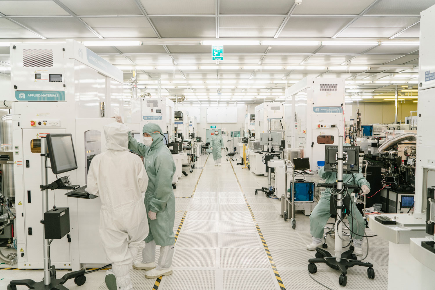
EPIC Advanced Packaging Center
Innovation and Commercialization
The EPIC Advanced Packaging Center in Singapore is designed to accelerate innovation and commercialization of advanced packaging technologies and marks the next phase of building out Applied’s global EPIC Platform.
The center brings together the necessary components to enable the next generation of energy-efficient computing for the AI era and builds upon the strong foundation of the Advanced Packaging Development Center (APDC), a decade-long collaboration between Applied Materials and Singapore’s Institute of Microelectronics (IME).
The EPIC Advanced Packaging Center innovation model will accelerate the time to innovation and shorten the time to commercialization.
Among the most advanced wafer-level packaging labs in the world, this facility enables innovation of the foundational building blocks of advanced packaging, including advanced bump and micro-bump, fine-line redistribution layer (RDL), TSV and hybrid bonding.
Dedicated Packaging Ecosystem
The center greatly expands Applied’s infrastructure for advanced packaging R&D and will include dedicated private spaces for customers and partners as well as a dedicated pilot line of packaging process equipment to enable test vehicles and prototype production.
-
EPIC Center Silicon Valley
-
EPIC Advanced Packaging Center
Rendering of the future Applied Materials Equipment and Process Innovation and Commercialization (EPIC) Center.
EPIC Center – Expected in 2026
The new Equipment and Process Innovation and Commercialization (EPIC) Center is planned as the heart of a high-velocity innovation platform designed to accelerate development and commercialization of the foundational technologies needed by the global semiconductor and computing industries. To be located at the Applied campus in Sunnyvale, California, the multibillion-dollar facility is designed to provide a breadth and scale of capabilities that is unique in the industry, including more than 180,000 square feet of state-of-the-art cleanroom for collaborative innovation with chipmakers, universities and ecosystem partners. Designed from the ground up to accelerate the pace of introducing new manufacturing innovations, the new EPIC Center is expected to reduce the time it takes the industry to bring a technology from concept to commercialization by several years, while simultaneously increasing the commercial success rate of new innovations and the return on R&D investments for the entire semiconductor ecosystem.
Innovation and Commercialization
The EPIC Advanced Packaging Center in Singapore is designed to accelerate innovation and commercialization of advanced packaging technologies and marks the next phase of building out Applied’s global EPIC Platform.
The center brings together the necessary components to enable the next generation of energy-efficient computing for the AI era and builds upon the strong foundation of the Advanced Packaging Development Center (APDC), a decade-long collaboration between Applied Materials and Singapore’s Institute of Microelectronics (IME).
The EPIC Advanced Packaging Center innovation model will accelerate the time to innovation and shorten the time to commercialization.
Among the most advanced wafer-level packaging labs in the world, this facility enables innovation of the foundational building blocks of advanced packaging, including advanced bump and micro-bump, fine-line redistribution layer (RDL), TSV and hybrid bonding.
Dedicated Packaging Ecosystem
The center greatly expands Applied’s infrastructure for advanced packaging R&D and will include dedicated private spaces for customers and partners as well as a dedicated pilot line of packaging process equipment to enable test vehicles and prototype production.