Products & Technologies
Products & Services
Company
Contact
Products & Services
Products & Technologies
Services
Resources
Company
Contact
Collaboration
Collaboration
Innovation Centers
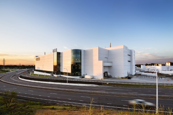
Maydan Technology Center
The Maydan Technology Center (MTC) is a billion-dollar, state-of-the-art facility dedicated to advanced chip making. With $100M reinvested each year to keep the center at the cutting edge, MTC is fine-tuned for rapid testing and development to accelerate our customers’ time to market. More than 500 Applied engineers work 24/7 alongside customers to bring new semiconductor designs to life.
MTC is the heart of Applied’s innovation engine. This unique center allows us to collaborate from the very beginning of the design process—often two generations ahead of current technologies—to expand what’s possible. MTC is both a fab and a test lab—allowing customers to test each manufacturing step under one roof. With over 120 advanced process tools ranging from lithography to deposition and etch, as well as 80 metrology and inspection tools, the center provides customers with a unique capability to speed transitions to new technologies, shorten cycle times to production and bring new products to market with reduced risk.
Materials Engineering Technology Accelerator (META)
Increasing Collaboration and Speed from Materials to Systems
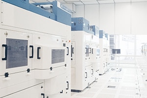
The Materials Engineering Technology Accelerator (META Center) is a new world-class hub for innovation in materials engineering research and development (R&D). The META Center speeds customer availability of new chipmaking materials and process technologies that enable breakthroughs in semiconductor performance, power, and cost, creating new ways for Applied and its customers to drive innovation as classic Moore’s Law scaling becomes more challenging.
The Center can also support industrial initiatives in the fields of Artificial Intelligence (AI), Augmented and Virtual Reality (AR/VR), advanced optics, big data, life sciences, and autonomous vehicles, among others, with advanced materials-based R&D, process technologies, device prototyping and pilot scale production capabilities.
This first-of-its-kind facility is furnished with a broad suite of Applied’s most advanced process systems along with complementary technologies needed for new chip materials and structures. The META Center is located in Albany, New York.
COLLABORATION NEWS
05.26.22 Applied Materials' New Ioniq PVD System
04.21.22 Applied Materials Technologies Enable 2D Scaling with EUV and 3D Gate-all-around Transistors