Products & Technologies
Products & Services
Company
Contact
Products & Services
Products & Technologies
Services
Resources
Company
Contact
In the Industry
Upcoming Events
Past Events
In the Community
Upcoming Events
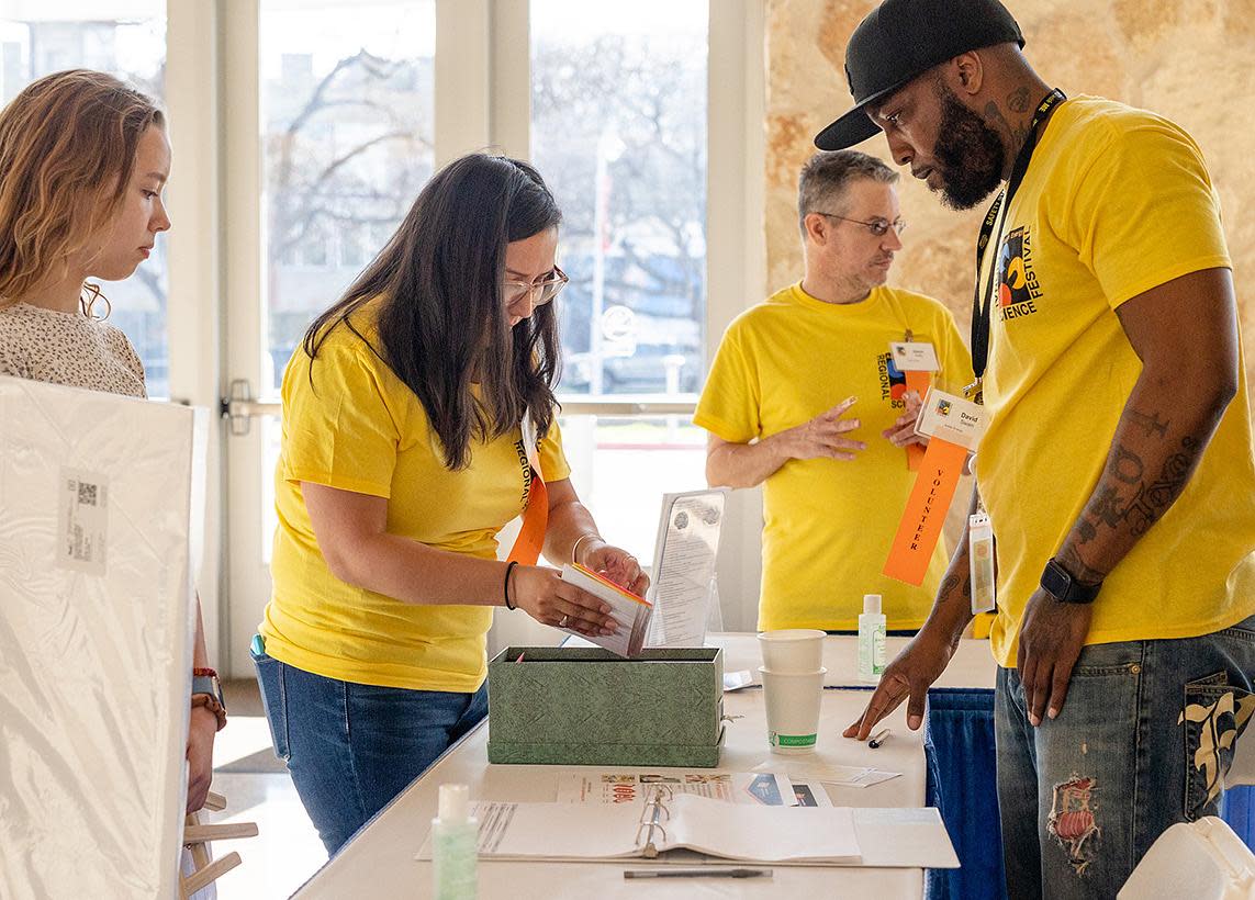
Greater Austin Regional Science & Engineering Fair
The Greater Austin Regional Science and Engineering Fair is a competition for students from 30 school districts and 14 counties who are advancing from their local schools. Volunteers can help out with tasks such as registration, parking and unloading, setup, ribbon hanging, logistics, etc.
Past Events
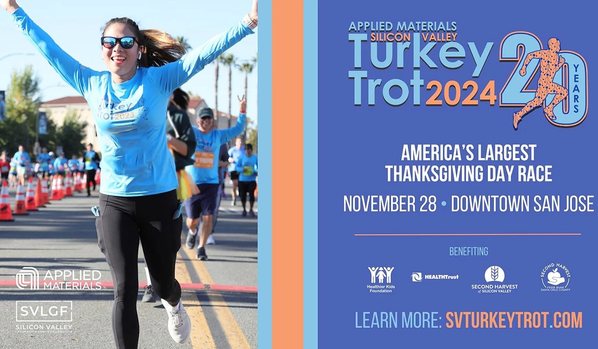
Applied Materials Silicon Valley Turley Trot
The Applied Materials Silicon Valley Turkey Trot is the largest Thanksgiving Day race in America and, in 2022, was the largest race in California. It allows participants to start Thanksgiving Day off on the right foot by celebrating generosity and wellness with a diverse group of runners and walkers committed to investing in their community.